Products
MEMS
Optics
Metrology & Inspection
Laboratory
Remanufacture
R&D
Spare Parts
Supports
Service
OEM
ODM
Testing
Training
Leasing
Applications
MEMS
Optics
Other
Suppliers
Company
Contact
CN
中文
English
Products
MEMS
Optics
Metrology & Inspection
Laboratory
Remanufacture
R&D
Spare Parts
Supports
Service
OEM
ODM
Testing
Training
Leasing
Applications
MEMS
Optics
Other
Suppliers
Company
Contact
Search
光刻机EN
涂胶显影EN
掩膜版EN
大标题第一行--en
第二行阿凡达范德萨发
先进半导体设备销售商,先进半导体设备销售商,先进半导体设备销售商,
先进半导体设备销售商,先进半导体设备销售商,
先进半导体设备销售商,EN
View All
Products
View All
MEMS
Optics
Metrology & Inspection
Laboratory
Remanufacture
R&D
Spare Parts
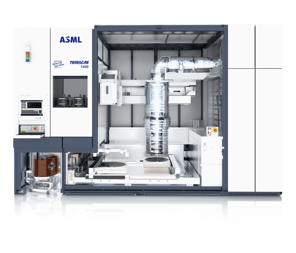
ASML TwinScan XT:1400F Refurbished
TwinScan XT:1400F DUV Lithography, The XT:1400F is a dual-stage ArF lithography system designed for 200mm and 300mm wafers at 65nm resolution.
JEOL JBX-3200MVS Electron Beam Lithography System
JBX-3200MVS is a variable-shaped electron beam lithography system for mask making of 32 nm to 28 nm nodes. Its advanced technology achieves high speed, high precision and high reliability. This EB system uses a variable-shaped 50 kV electron beam and a step-and-repeat specimen stage.
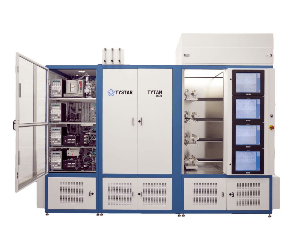
Tystar Tytan Mini LPCVD
Tytan Mini Furnace Systems are designed for diffusion, oxidation and LPCVD applications.
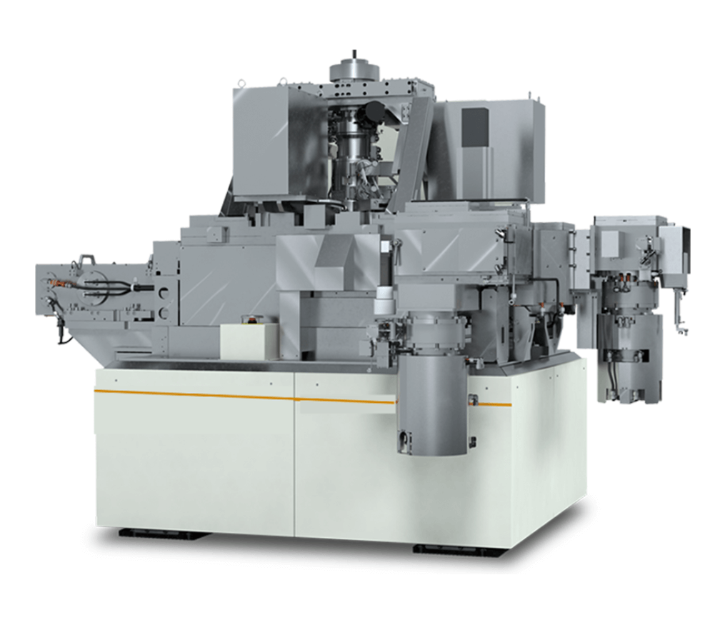
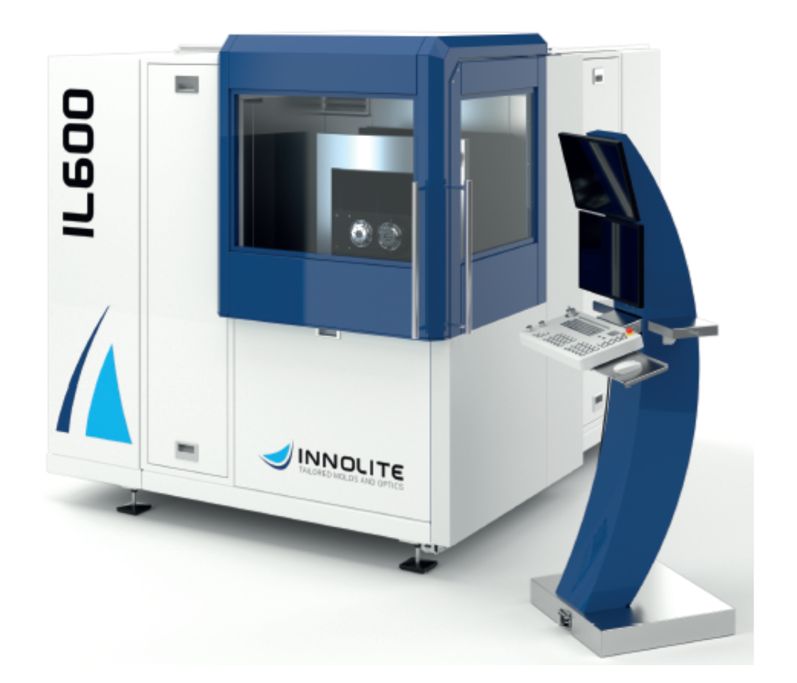
IL600 UP Machining Center
The IL600 is a four-axis or optional five-axis ultra-precision machining center that enables high-productivity optical product machining.
Supports
View All
Service
Service Service Service
View All
OEM
OEM OEM OEM
View All
ODM
ODM ODM ODM
View All
Applications
View All
MEMS
Optics
Other
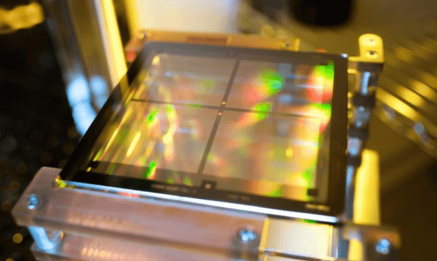
Photomask (Reticle)
A photomask (also simply called a mask) is an opaque plate with transparent areas that allow light to shine through in a defined pattern. Photomasks are commonly used in photolithography for the production of integrated circuits (ICs or "chips") to produce a pattern on a thin wafer of material (usually silicon). In semiconductor manufacturing, a mask is sometimes called a reticle.
View Detail
2025.04.22
View Detail
2025.03.18
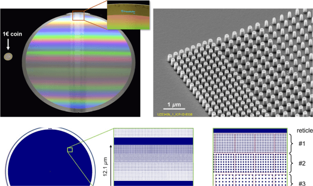
Potential of E-beam lithography for micro- and nano-optics fabrication on large areas
The availability of high-resolution and high-throughput lithographic fabrication technologies, such as electron-beam lithography, based on variable shaped beam writing and character projection opens the way for the flexible use of various optical nano-structures for some of the most demanding applications. We discuss the technical features, advantages, and limitations of these pattering approaches and show how they can favorably be combined to realize optical nano-structures for applications, which are as diverse as gratings for ultra-short laser pulses or high-resolution spectrometers, computer generated holograms for asphere testing, various optical meta-structures (lenses and gratings), or UV-polarizers.
View Detail
2025.04.17
Suppliers
View All